반도체 장비
㈜힘스의 반도체장비 제품소개입니다.
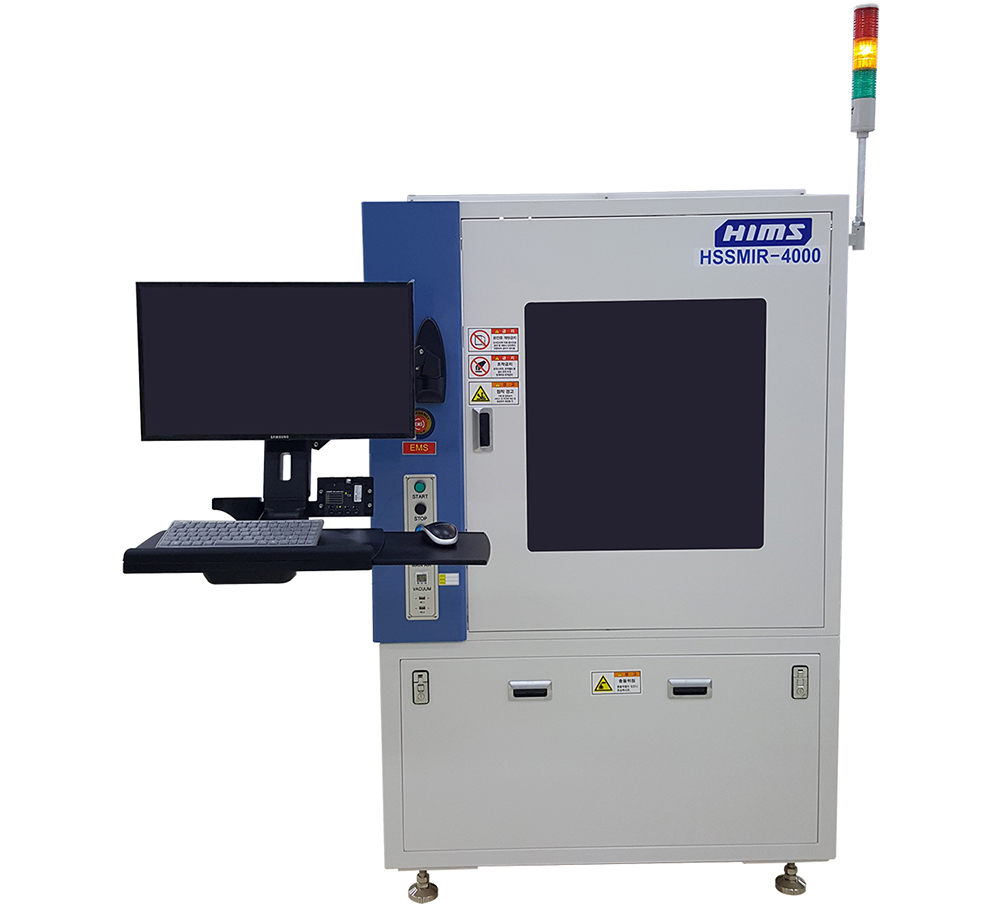
IR Die Inner Crack Inspection System Model No. HSSMIR-4000
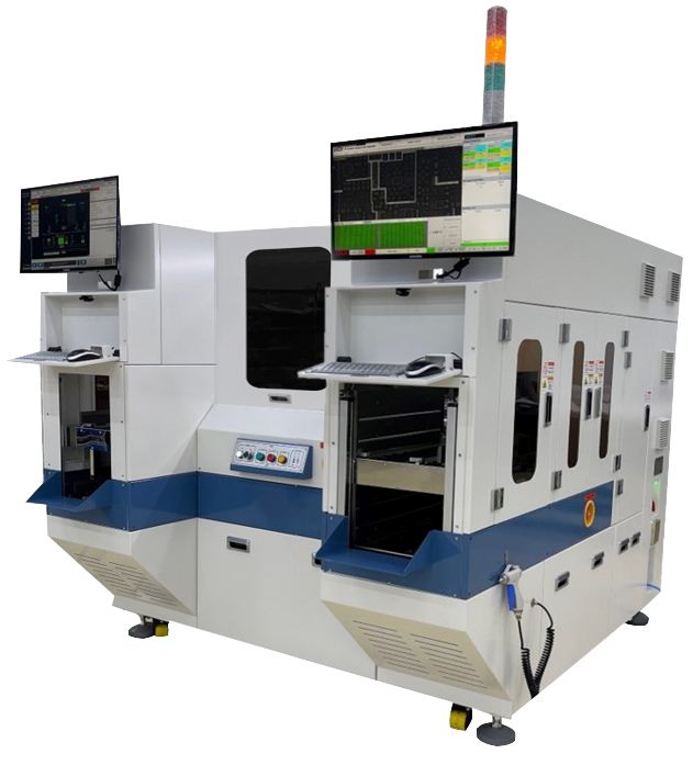
힘스 반도체용 적외선 검사기는 산업용 적외선을 이용하여 반도체칩 내부의 결함을 감지하는 기술입니다.
최고사양의 비전시스템과 자체개발 검사 알고리즘 적용으로 검사 정확성 및 생산성이 비약적으로 향상되었습니다. 본 설비는 ‘PCB Strip’형태의 자재를 처리할 수 있도록 설계되어 있습니다.
Specification
| Category | Item | Unit | Specification | Remark |
|---|---|---|---|---|
| Vision system | Inspection items | - | Inner crack & Damage | Surface defect detection available |
| Vision system | Camera | - | line scan type, NIR [Near InfraRed] | SWIR camera available |
| Vision system | Illumination | - | Halogen IR lamp | - |
| Equipment | Handling system | - | Conveyor type | - |
| Equipment | Foot Print | Mm | 1,980x1,700x1,800 | adaptable item |
| Equipment | Weight | Ton | 2 | adaptable item |
| Equipment | Cleanness | Class | 100 | 0.5um |
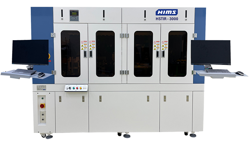
IR & Tray AVI Machine Model No. HSTIR-3000
힘스 반도체용 적외선 검사기는 산업용 적외선을 이용하여 반도체칩 내부의 결함을 감지하는 기술입니다. 최고사양의 비전시스템과 자체개발 검사 알고리즘 적용으로 검사 정확성 및 생산성이 비약적으로 향상되었습니다.
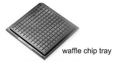
본 설비는 ‘Waffle Chip tray’을 핸들링하고 IR 검사를 수행할 수 있는 기술이 적용되어 있습니다.
Specification
| Category | Item | Unit | Specification | Remark |
|---|---|---|---|---|
| Vision system | Inspection items | - | Inner crack & Damage | Surface defect detection available |
| Vision system | Camera | - | line scan type, NIR [Near InfraRed] | SWIR camera available |
| Vision system | Illumination | - | Halogen IR lamp | - |
| Equipment | Handling system | - | Turn table type | 2” ~ 4” chip tray |
| Equipment | Foot Print | Mm | 2,500x1,800x1,800 | adaptable item |
| Equipment | Weight | Ton | 3.5 | adaptable item |
| Equipment | Cleanness | Class | 100 | 0.5um |
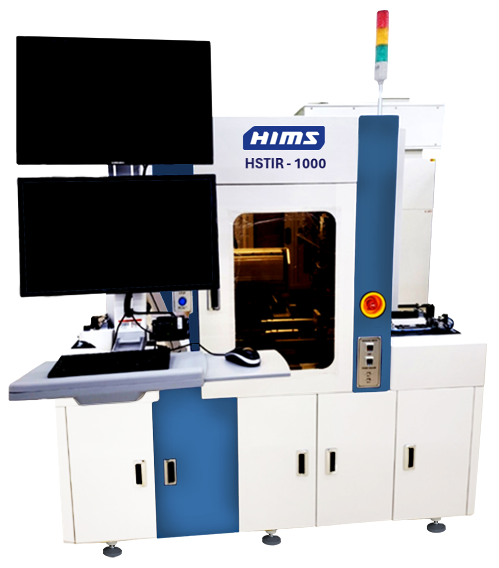
Tray (Unit Base) IR Crack Inspection System Model No. HSTIR-1000
힘스 반도체용 적외선 검사기는 산업용 적외선을 이용하여 반도체칩 내부의 결함을 감지하는 기술입니다.
최고사양의 비전시스템과 자체개발 검사 알고리즘 적용으로 검사 정확성 및 생산성이 비약적으로 향상되었습니다.
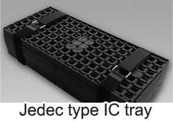
본 설비는 ‘Jedec type IC tray’을 핸들링하고 IR 검사를 수행할 수 있는 기술이 적용되어 있습니다.
Specification
| Category | Item | Uni | Specification | Remark |
|---|---|---|---|---|
| Vision system | Inspection items | - | Inner crack & Damage | Surface defect detection available |
| Vision system | Camera | - | line scan type, NIR [Near InfraRed] | SWIR camera available |
| Vision system | Illumination | - | Halogen IR lamp | - |
| Equipment | Handling system | - | Conveyor type | Tray transfer |
| Equipment | Foot Print | Mm | 1,210 x 1,750 x 1,760 | adaptable item |
| Equipment | Weight | Ton | 1.5 | adaptable item |
| Equipment | Cleanness | Class | 100 | 0.5um |
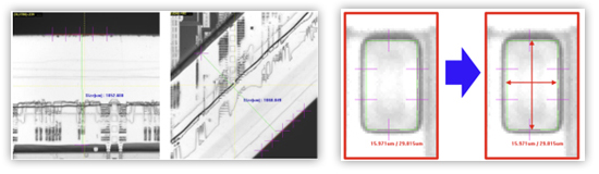
Overlay Inspection System
㈜힘스의 Overlay Inspection System은 여러 층으로 구성된 반도체 칩에서 레이어 간의 정렬 오차를 측정하고 조정하는데 중요한 역할을 합니다.
본 장비는 각 레이어가 정확하게 정렬되도록 하여, 반도체 소자의 성능과 수율을 높이는데 필수적인 장비입니다.
Specification
| Subject | Item | Specification | Note |
|---|---|---|---|
| System Configuration | Wafer Type | ~300mm(Notch) | - |
| System Configuration | Cassette Type | 25 Wafers Cassette / Foups | SEMI compliant |
| System Configuration | No. of Stage or Load port | 2 Ports | - |
| System Configuration | 3D Measurement system | WSI | White light Scanning Interferometry |
| System Configuration | Host Communication (SECS-GEM) |
Applied | - |
| System Configuration | Cleanness | Class 100 | - |
| 2D Vision System | Sensitivity | 20x / 0.3㎛ | Alignment / EBR 측정용 – 5x/2.5x 3D 측정용 – 20x |
| 2D Vision System | Sensitivity | 5x / 0.5㎛ | |
| 2D Vision System | Sensitivity | 2.5x / 1㎛ | |
| 3D Vision System | Resolution | 1.5nm | 독립기초 기준 |
| 3D Vision System | Repeatability | <0.25㎛ @ 3Sigma | |
| 3D Vision System | Range | 20㎛ ~ 380㎛ | - |
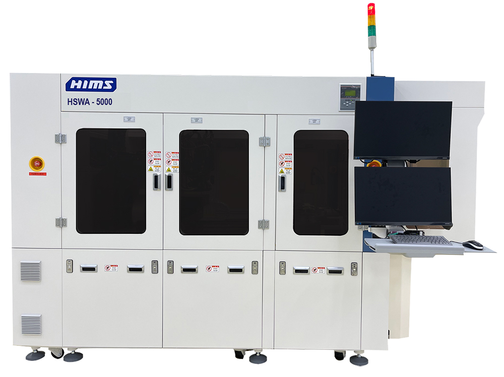
Wafer Bump Inspection System Model No. HSWA – 5000
2D Mono Camera 사용하여 웨이퍼의 외관 결함 및 계측이 가능한 시스템입니다.
향상된 외관 검사와 Pad 사이즈 및 웨이퍼의 끝부분 노출(Edge Exposure) 검사 등 계측 기능도 수행 가능한 모델입니다.
XY 스테이지의 이동 효율성 향상 및 고속 트리거 생성 그리고 알고리즘 처리속도를 높여 검사 시간을 획기적으로 단축하였습니다. 또한, SPC 및 RMS와 같은 향상된 생산 및 분석 도구를 제공하여 수율 및 불량 분석을 도와주고, 생산성 향상을 제공합니다.
Specification
| Category | Item | Unit | Specification | Remark |
|---|---|---|---|---|
| Vision system | Wafers | Inch | Max 12” | - |
| Vision system | Inspection items | - | Defects on wafer surface | - |
| Vision system | Camera | - | 2D, Area Scan | 3D available |
| Equipment | Handling system | - | Double Arm robot | Bare / Framed wafer |
| Equipment | Foot Print | Mm | 2,580 x 1,400 x 2,309 | adaptable item |
| Equipment | Weight | Ton | 1.5 | adaptable item |
| Equipment | Cleanness | Class | 100 | 0.5um |
2D/3D_AOI System Model No. HSSM-2000/2100
2D/3D 카메라를 이용하여 칩 및 컴포넌트 등의 외관 검사 설비.
컴포넌트, 솔더 이상, 칩 이상, 이물 등의 2D 검사 포함하여 컴포넌트 및 다이 기울임 이상 등의 3D 검사도 수행 가능함
Specification
| Items | Unit | 2D Vision (HSSM-2100) | 3D Vision (HSSM-2000) | Remark |
|---|---|---|---|---|
| Camera | - | Area Scan | Line Scan | |
| Material movement | - | From Left side to right side | Dual lane | |
| Foot print | mm | 1020 x 1400 x 1733+202(PC) | 1680 x 1330 x 1787+202(PC) | Length x Width x Height |
| Weight | ton | About 1 ton | About 1.5 ton | |
| Power supply | - | 220V/50~60Hz/3Phase | ||
Pellicle Inspection System Model No. CPI-300(PS)
CPI-300(PS)시스템은 Lithographic Photo-mask 공정을 위하여 Reticle의 상부(Glass Side)와 하부(Pellicle Side)표면의 결함을 검사하는 시스템입니다.
Specification
| Category | Item | Unit | Specification | Remark |
|---|---|---|---|---|
| Vision system | Inspection items | - | ≥4.0 Defects : G&I, DUV, KrF, ArF of Binary / PSM | - |
| Vision system | Repeatability | % | ≥97% SPL | |
| Vision system | Pixel Resolution | ㎛ | 2.8 | |
| Vision system | Light Source | - | White LED | |
| Vision system | Inspection area | - | Inspect 6 Inch Reticle | - |
| Vision system | Throughput | Sec | 80sec, simultaneous scan (Including loading and align) |
According to vision system |
| Equipment | Foot Print | Mm | 814 x 345 x 728 | Module type |
| Equipment | Material used Surface finished |
- | Stainless Steel – Anodized Aluminum – ESD Safe Synthetic Material | |
| Equipment | Weight | kg | 117 |
HIMS AI SYSTEM – HAIF(Hims AI Framework)
㈜힘스의 ‘HAIF’는 Hims AI Framwork로 자체 개발한 자사 AI 시스템 입니다.
Machine Learning(AI)를 이용해 검사, 학습, 적용, 결과 보고, 관리를 위한 통합 Framework 입니다.

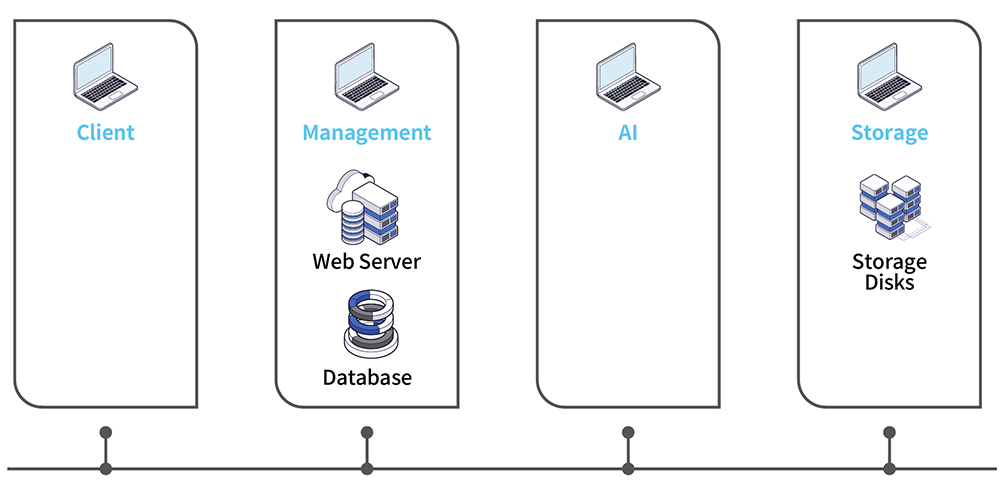
- 룰 기반 검사프로그램과 네트워크를 통한 직접적인 통신
- Web page를 통한 User Interface 지원
- AI 검사/학습/적용/관리를 위한 통합 Framework
- OS : Linux, Windows 모두 지원
- Language : C++, C#, Python, NodeJS 모두 지원
