Semiconductor
Here are our main products on semiconductor field.
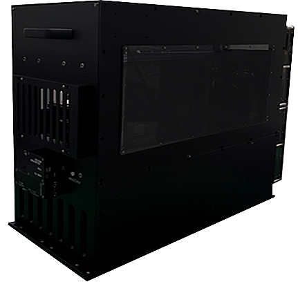
IR Die Inner Crack Inspection System Model No. HSSMIR-4000
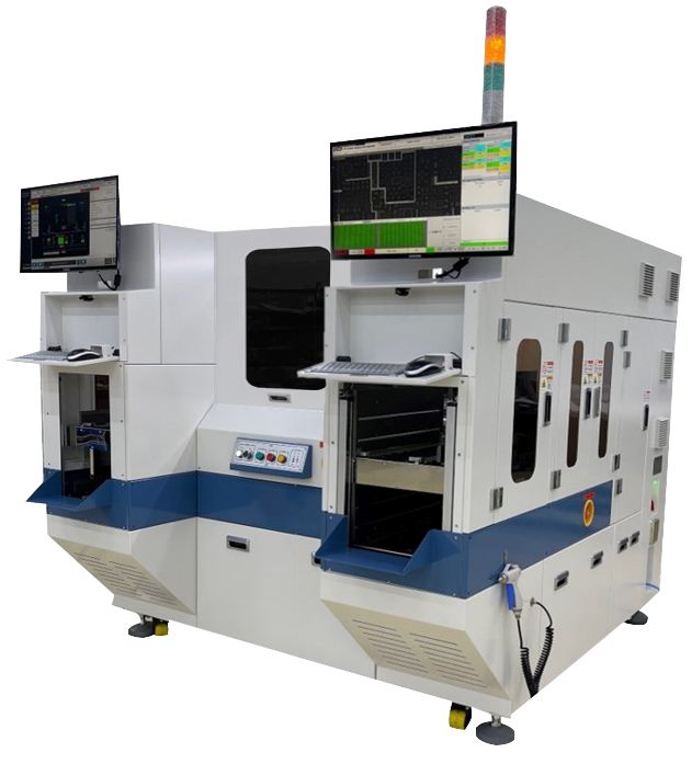
HIMS semiconductor IR inspection machine use industrial infrared rays to detect defects inside semiconductor chips.
With the application of the highest-performance vision system and self-developed inspection algorithms, the inspection accuracy and productivity have been significantly improved.
This equipment is designed to handle ‘PCB Strip’.
Specification
| Category | Item | Unit | Specification | Remark |
|---|---|---|---|---|
| Vision system | Inspection items | - | Inner crack & Damage | Surface defect detection available |
| Vision system | Camera | - | line scan type, NIR [Near InfraRed] | SWIR camera available |
| Vision system | Illumination | - | Halogen IR lamp | - |
| Equipment | Handling system | - | Conveyor type | - |
| Equipment | Foot Print | Mm | 1,980x1,700x1,800 | adaptable item |
| Equipment | Weight | Ton | 2 | adaptable item |
| Equipment | Cleanness | Class | 100 | 0.5um |
IR & Tray AVI Machine Model No. HSTIR-3000
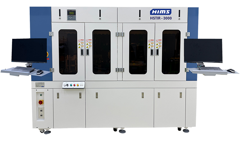
HIMS semiconductor IR inspection machine use industrial infrared rays to detect defects inside semiconductor chips.
With the application of the highest-performance vision system and self-developed inspection algorithms, the inspection accuracy and productivity have been significantly improved.
This equipment is designed to handle and to inspect chips on ‘waffle chip tray’.
Specification
| Category | Item | Unit | Specification | Remark |
|---|---|---|---|---|
| Vision system | Inspection items | - | Inner crack & Damage | Surface defect detection available |
| Vision system | Camera | - | line scan type, NIR [Near InfraRed] | SWIR camera available |
| Vision system | Illumination | - | Halogen IR lamp | - |
| Equipment | Handling system | - | Turn table type | 2” ~ 4” chip tray |
| Equipment | Foot Print | Mm | 2,500x1,800x1,800 | adaptable item |
| Equipment | Weight | Ton | 3.5 | adaptable item |
| Equipment | Cleanness | Class | 100 | 0.5um |
Tray (Unit Base) IR Crack Inspection System Model No. HSTIR-1000
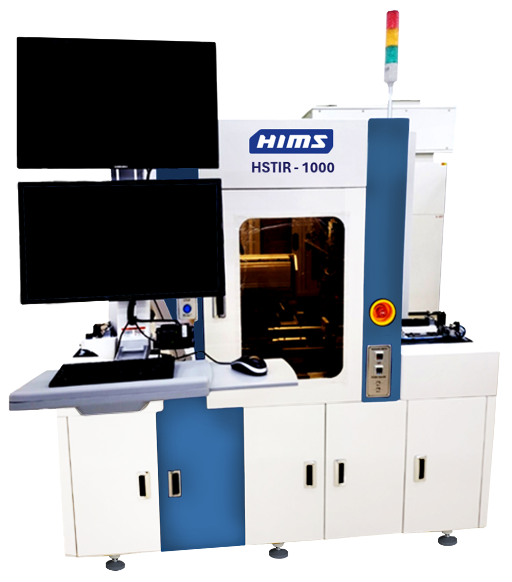
HIMS semiconductor IR inspection machine use industrial infrared rays to detect defects inside semiconductor chips.
With the application of the highest-performance vision system and self-developed inspection algorithms, the inspection accuracy and productivity have been significantly improved.
This equipment is designed to handle and to inspect chips on ‘Jedec type IC tray’.
Specification
| Category | Item | Uni | Specification | Remark |
|---|---|---|---|---|
| Vision system | Inspection items | - | Inner crack & Damage | Surface defect detection available |
| Vision system | Camera | - | line scan type, NIR [Near InfraRed] | SWIR camera available |
| Vision system | Illumination | - | Halogen IR lamp | - |
| Equipment | Handling system | - | Conveyor type | Tray transfer |
| Equipment | Foot Print | Mm | 1,210 x 1,750 x 1,760 | adaptable item |
| Equipment | Weight | Ton | 1.5 | adaptable item |
| Equipment | Cleanness | Class | 100 | 0.5um |
Wafer Bump Inspection System Model No. HSWA – 5000
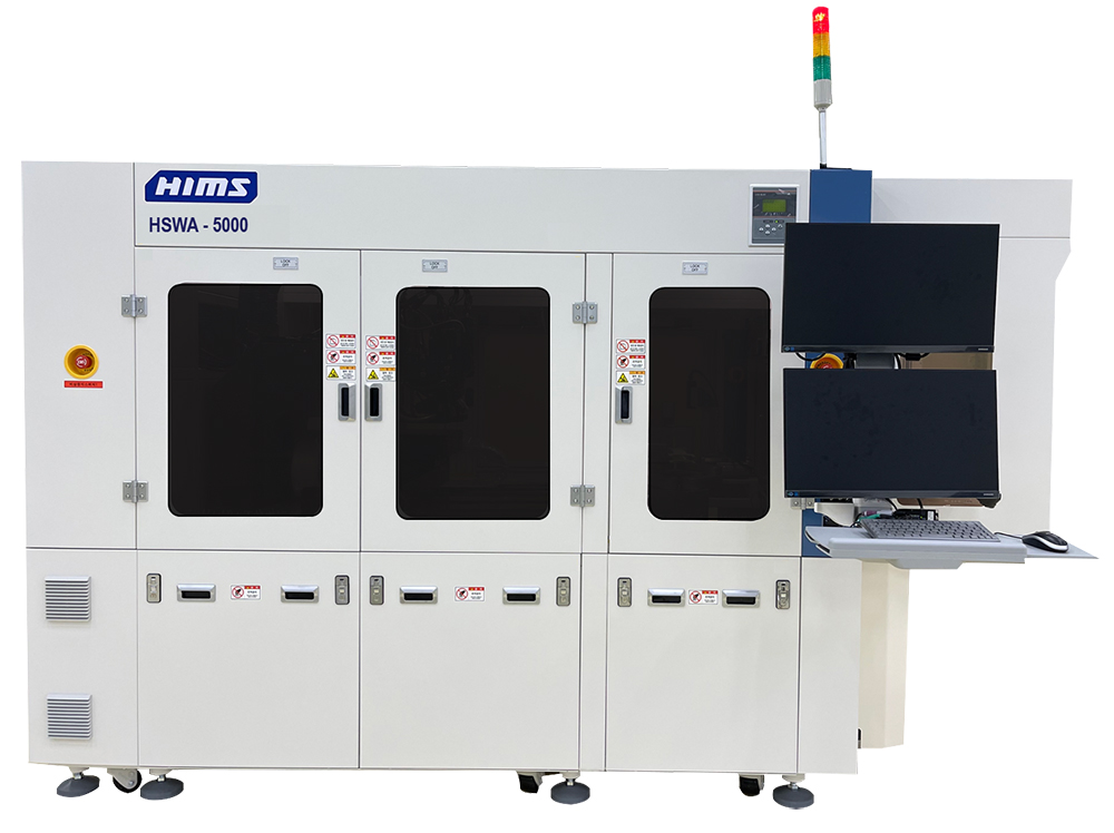
HIMS wafer bump inspection system uses a 2D mono camera to detect wafer defects and perform measurements. It is a model that can perform both enhanced appearance inspection and measurements, such as pad size and wafer edge exposure inspection.
We have significantly reduced inspection time by improving the movement efficiency of the XY stage, generating high-speed triggers, and increasing the algorithm processing speed.
In addition, we provide improved production and analysis tools such as SPC and RMS to help with yield and defect analysis and improve productivity.
Specification
| Category | Item | Unit | Specification | Remark |
|---|---|---|---|---|
| Vision system | Wafers | Inch | Max 12” | - |
| Vision system | Inspection items | - | Defects on wafer surface | - |
| Vision system | Camera | - | 2D, Area Scan | 3D available |
| Equipment | Handling system | - | Double Arm robot | Bare / Framed wafer |
| Equipment | Foot Print | Mm | 2,580 x 1,400 x 2,309 | adaptable item |
| Equipment | Weight | Ton | 1.5 | adaptable item |
| Equipment | Cleanness | Class | 100 | 0.5um |
Pellicle Inspection System Model No. CPI-300(PS)
The CPI-300(PS) system is a system that inspects defects on the upper (Glass Side) and lower (Pellicle Side) surfaces of the reticle for the lithographic photo-mask process.
Specification
| Category | Item | Unit | Specification | Remark |
|---|---|---|---|---|
| Vision system | Inspection items | - | ≥5.0 Defects:G / IDUV,KrF,ArfofBinary / PSM | - |
| Vision system | Repeatability | % | ≥97% SPL | |
| Vision system | Light Source | - | Cool White LED | |
| Vision system | Inspection area | - | inspect 6 inch reticle | - |
| Equipment | Foot Print | Mm | 828 × 356× 732 | Module type |
| Equipment | Material used & surface finished | - | Stainless Steel- Anodized Aluminum- ESD safe synthetic material |
2D/3D_AOI System Model No. HSSM-2000/2100
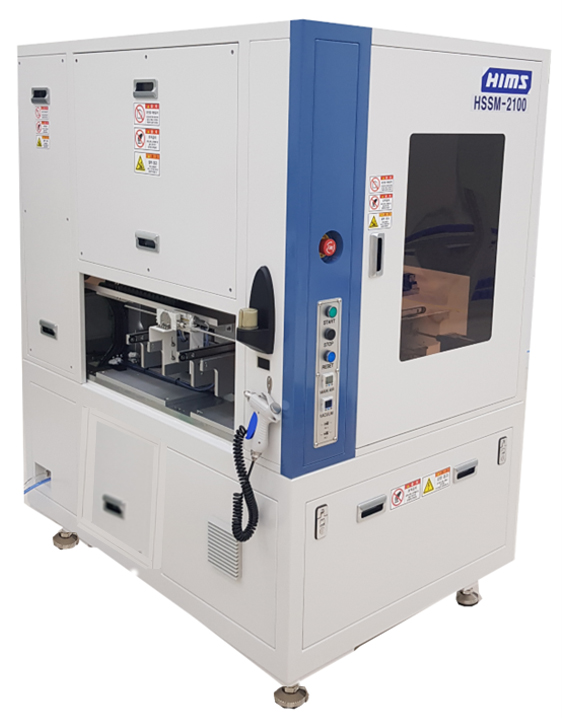
AOI system that uses 2D/3D cameras to inspect the aspect of chips and components.
It is available to perform 2D inspections of components, solder defects, chip defects, and foreign materials, as well as 3D inspections of components and die abnormal tilt.
Specification
| Items | Unit | 2D Vision (HSSM-2100) | 3D Vision (HSSM-2000) | Remark |
|---|---|---|---|---|
| Camera | - | Area Scan | Line Scan | |
| Material movement | - | From Left side to right side | Dual lane | |
| Foot print | mm | 1020 x 1400 x 1733+202(PC) | 1680 x 1330 x 1787+202(PC) | Length x Width x Height |
| Weight | ton | About 1 ton | About 1.5 ton | |
| Power supply | - | 220V/50~60Hz/3Phase | ||
